

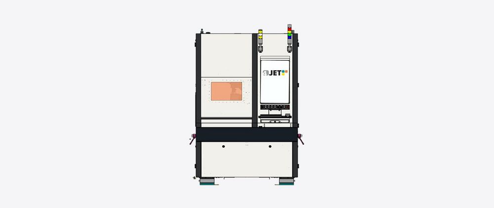
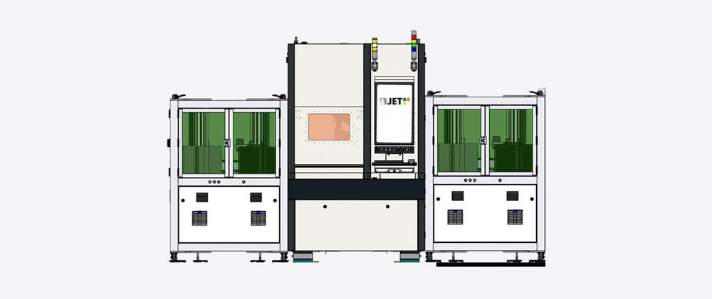
PEARL 400S – The Modular Solution for High-End Glass Processing
The PEARL 400S is a modular laser processing platform for glass wafers, glass substrates for the semiconductor industry, and other brittle materials.
It is ideal for applications in microelectronics, optics, sensing, and AR technology – anywhere where the highest precision, process reliability, and cleanroom compatibility are required.
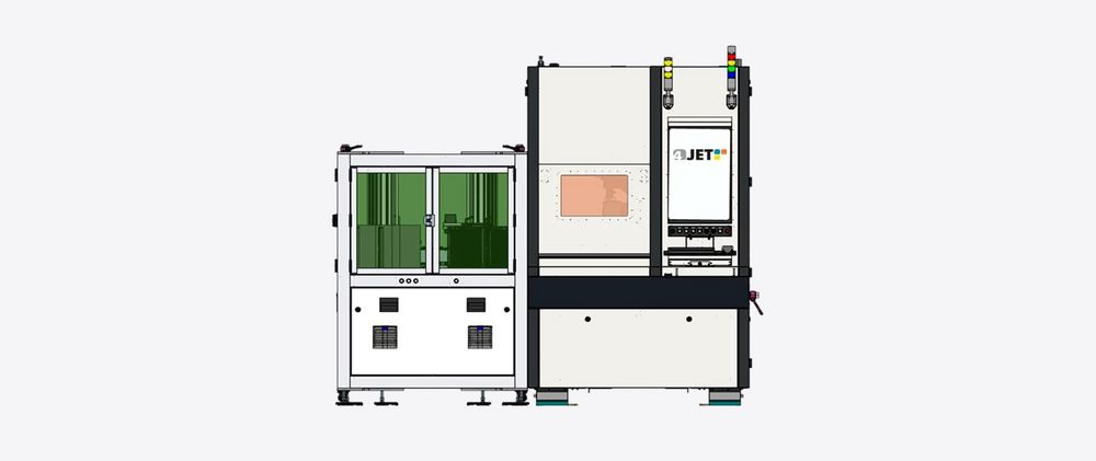
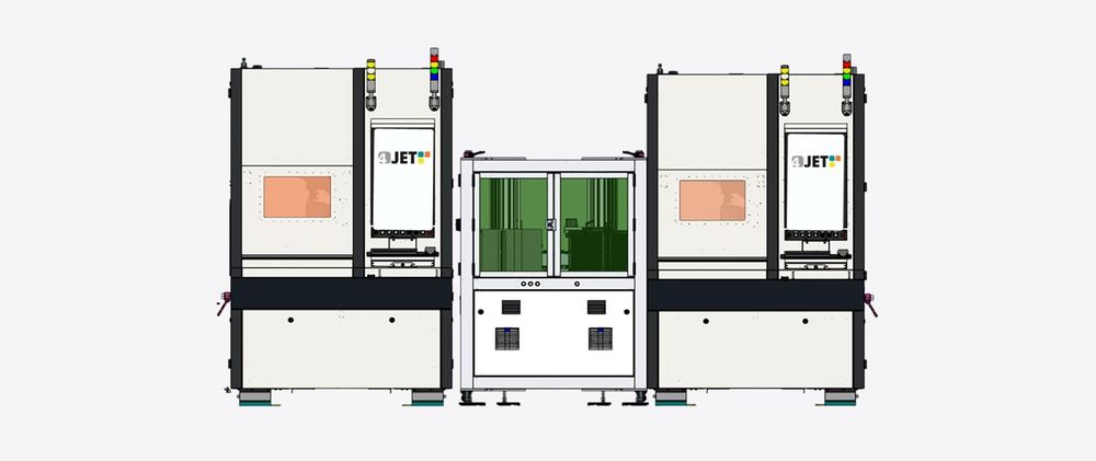
The platform is built on a highly stable granite gantry and is available in various configurations – each optimized for specific process steps such as nanoPerforation (Wafer Dicing, WD), thermal separation (WS), ablation, or microdrilling (Wafer Ablation, WA).
- Glass Wafers for MEMS and Sensing
Processing glass wafers for micro-electromechanical systems (MEMS), pressure sensors, accelerometers, and other sensing technologies.
- Micro-Optics & Wafer Level Optics (WLO)
Structuring and singulation of micro-optical components at wafer level, including stacked wafers for complex optical systems.
- Macro- and Micro-Optics/Molded Optics
Precision processing of optical components in various sizes, including molded optics for industrial and medical applications.
- Meta-Surfaces for AR & Wearables
Structuring glass for advanced optical functions, for example AR glasses, head-up displays, and wearable devices.
- Rotary & Linear Encoders
High-precision structuring and singulation of glass and silicon components for position and motion sensing in automation.
- Research & Development/Prototyping
Precision drilling, structuring, and dicing for R&D projects, prototyping, and small series – adaptable to new materials and designs.
- Dicing of SiC and Glass
High-precision dicing of silicon carbide, hardened and non-hardened glass – even with challenging geometries and coatings.
- Dies with Coatings & Microstructures
Processing individual chips (dies) with functional layers, microstructures, or sensitive surfaces – without damage.
- Color Filter and Filter Technologies
Structuring and dicing of color filters and optical coatings for cameras, sensors, and display technologies.
- Glass in Semiconductor Applications
Processing glass as a carrier material or optical interface in modern semiconductor applications (e.g., Co-Packaged Optics).
- Bio and medical technology
- Next Generation Sequencing (NGS): Structuring glass for DNA analysis platforms.
- Lab-on-a-chip & microfluidics: Production of microfluidic channels and structures on glass.
- DNA drug discovery: glass structures for drug discovery and screening.
- Microscopy accessories: Slide glasses and cover glasses – also with biofilms or functional coatings.
- Cuvettes & Flow Cells: Precise glass processing for optical measuring cells and flow chambers.
Highlights of the PEARL 400S Platform
Various Configurations Are Possible
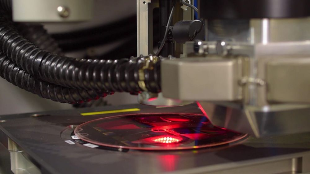
PEARL 400S WD – Laser Dicing for Glass Wafers
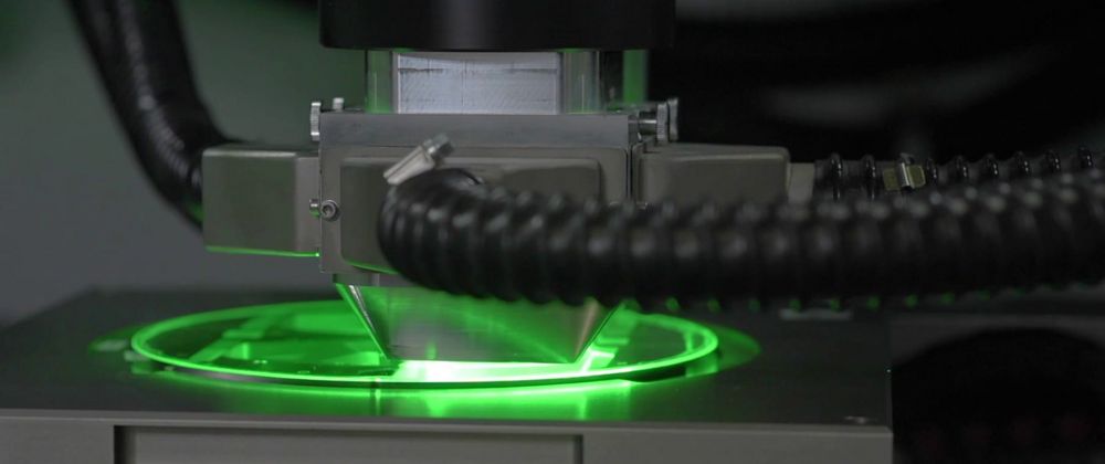
The WD version (Wafer Dicing) is designed for laser cutting of glass wafers and brittle materials, performing the first stage – nanoPerforation – to prepare the substrate for separation.
The separation process in two steps:
1. nanoPerforation
A picosecond laser creates a series of microscopic modifications in the glass volume along the desired separation contour.
2. Separation
Takes place in a separate process step, either:
- Thermally with the PEARL 400S WS, or
- Mechanically with the DTX 200 NX, a high-precision breaking system.
Whether small dies or large optics and eyepieces – the WD version covers a wide range of applications. Mechanical separation is the better choice for very small components (< 3 mm), sensitive functional layers that could be damaged by the heat-affected zone of a CO2 laser, or materials with low thermal expansion coefficients (e.g., lithium niobate, quartz glass). In all other cases, thermal separation can be used.
Advantages of the PEARL 400S WD
Two variants for maximum flexibility
We offer two variants of our patented nanoPerforation process:
nanoPerforation (nP)
the standard solution for precise, clean cuts with high process reliability.
Enhanced nanoPerforation (EnP)
with even higher edge strength, reduced chipping, and greater geometric flexibility – ideal for complex cutting patterns and industrial high-throughput applications.
Detailed information on the technology and areas of application can be found on our application page for laser glass cutting.
PEARL 400S WA – Laser Ablation & Microprocessing for glass and brittle materials
The WA version (Wafer Ablation) is built for laser ablation, microdrilling, and surface structuring –contactless, stress-free, and with minimal heat-affected zones. It works with glass, silicon carbide (SiC), and coated substrates.
Typical applications:
Precise micro-drilling with minimal chipping and high edge quality.
For meta-surfaces, optical components, and microfluidic systems.
For functionalization or preparation for further process steps, for example.
Even below 100 µm, without mechanical stress.
Detailed information on glass processing by drilling and structuring can be found on our application page for laser drilling.
Advantages:
Common technical data (WD & WA)
| Category | Feature | Specification |
|---|---|---|
| System Size & Weight | Dimensions (W × D × H) With wafer handler | 1400 × 1400 × 2380 mm 2600 x 1865 x 2380 mm |
| Weight Weight with handler | ~ 2,600 kg ~ 3,400 kg | |
| Axes & Motion | Processing Area | 400 × 400 mm |
| Feed Rate | Up to 1000 mm/s | |
| Acceleration | 10 m/s² | |
| Pattern Accuracy* | < 2.5 µm + 10 × 10⁻⁶ × L | |
| Repeatability | ≤ 1 µm | |
| Pattern Placement Accuracy | 10 µm | |
| Software & Operation | HMI | Touchscreen-based user interface |
| CAD Post-Processor | DXF import, easy job configuration | |
| cVision | Fiducial and glass edge recognition | |
| MES SECS/GEM (optional) | Manufacturing execution system integration | |
| Automation | Wafer Handler | Fully automated wafer handler for two cassettes |
| Wafer ID Reader | Automatic wafer ID reading |
Comparison of options
- Enhanced nanoPerforation
- Height Sensor
- Code Reader (2D)
- Wafer ID Reader
- Beam Profiler
- Ionizer
- Humidity booster
- Earthquake Protection
- Transformer
- Chiller (PCW)
- Remote Access (GenuBox)
- Height Sensor
- Code Reader (2D)
- Wafer ID Reader
- Beam Profiler
- Ionizer
- Earthquake Protection
- Transformer
- Chiller (PCW)
- Remote Access (GenuBox)


