


Wafer Dicing – Precision Scribing & Breaking
Wafer Dicing is the final process step in the manufacturing of chips, micro-optics, MEMS devices, and sensor components. It involves the singulation of wafers into individual chips with high precision.
Unlike conventional techniques such as laser cutting, blade dicing, or mechanical scribing, we count on a Breaking System tailored for precision wafer separation – especially in glass wafer dicing applications.
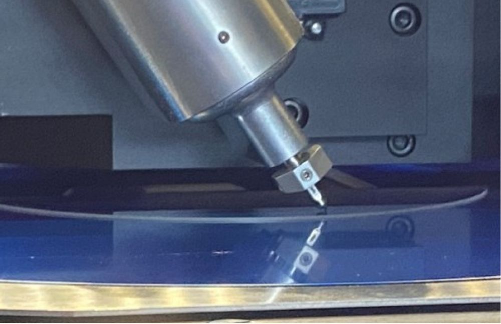
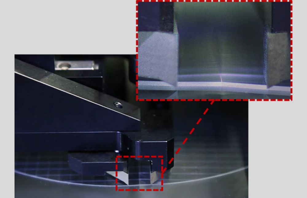
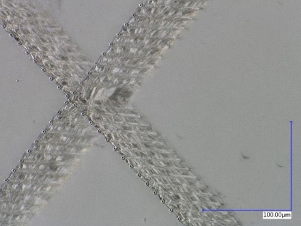
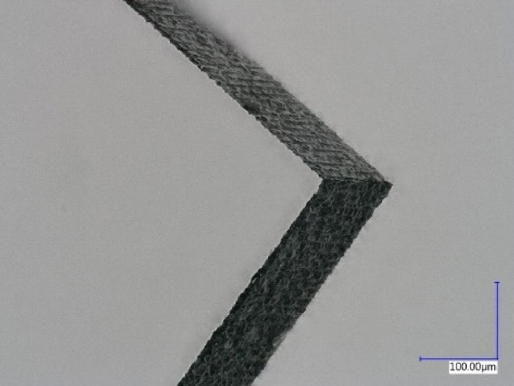
The Dry Dicing process starts with either laser scribing (nanoPerforation) or diamond scribing, where a controlled micro-crack is introduced into the wafer surface along defined lines. The DTX 200 NX then applies mechanical breaking to cleanly separate the wafer along these scribe lines.
For optimal singulation and ease of handling, the wafer – mounted on dicing tape – can be processed afterward with the DXE wafer expander, which gently stretches the tape to separate and stabilize the individual dies for downstream pick-and-place or inspection
This dry, contact-free process is ideally suited for thin glass, coated wafers, and sensitive compound semiconductors, delivering:
- Particle-free singulation without cooling liquids
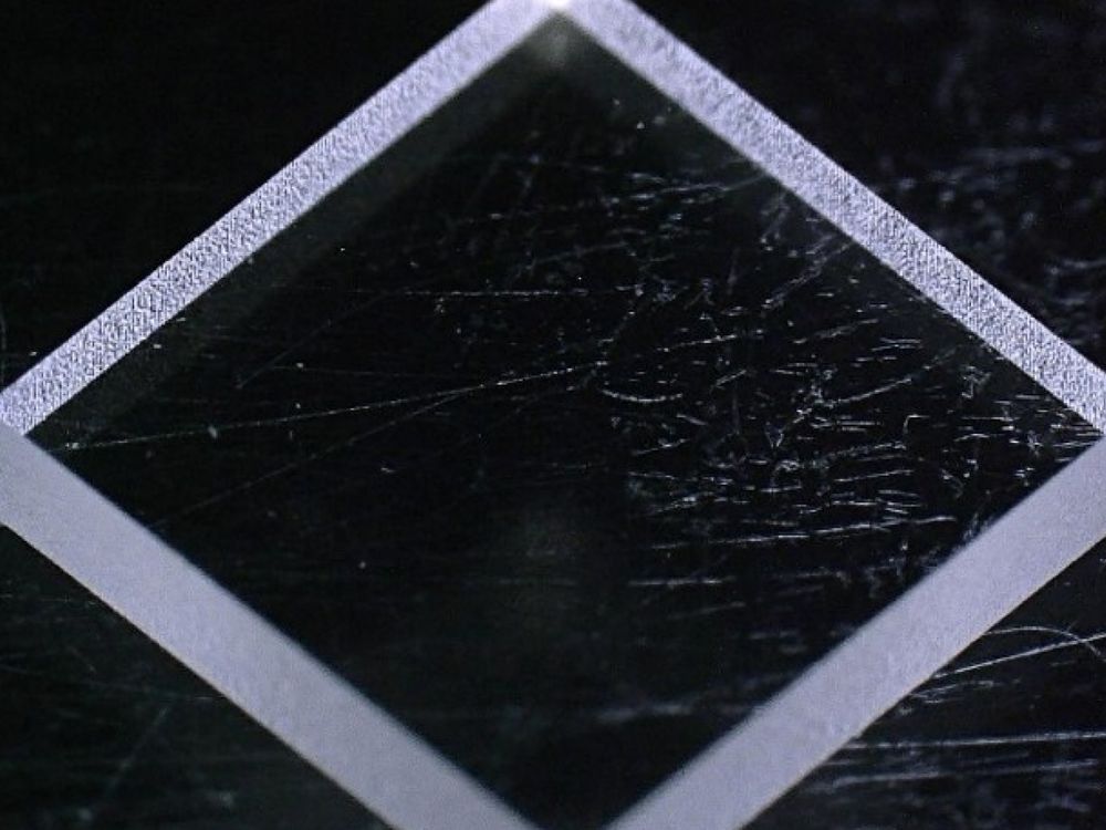
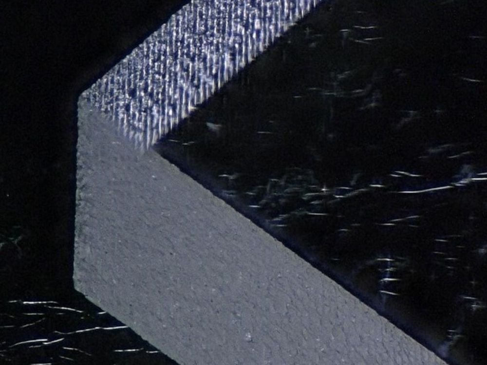
- High edge quality with minimal chipping
- No thermal damage or heat-affected zones
- Scalability for high-throughput manufacturing
- Excellent compatibility with ultra-thin glass and multilayer substrates
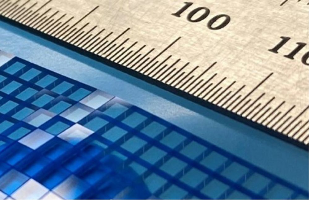
Compared to laser cutting, our scribe and break process allows for extremely small product sizes in the sub-mm range (nanoPerforation & Break) or singulation of non-transparent materials (Diamond Scribe & Break).
The Dry Dicing Process supports a wide range of advanced applications, including:
- Singulation of microfluidic chips from glass wafers
- Semiconductor wafer dicing, including silicon (Si), silicon carbide (SiC), and III-V materials like AlN and InP
- Precision dicing of photonic integrated circuits (PICs)
- Dicing of MEMS wafers and flat panel display substrates
- Wafer dicing of AR/VR optical components, often featuring complex coatings or delicate materials
Whether for prototyping or full-scale production, the DTX 200 NX delivers mechanical dicing of glass wafers with unmatched reliability and repeatability.
FAQ: Wafer Dicing Using the Scribe & Break Method
The Scribe & Break method is based on a two-step process:
- Scribing – A diamond tool or laser radiation creates a highly precise scribe line on the wafer.
- Breaking – The wafer is then cleanly broken along this predefined line.
Comparison with other methods:
- Mechanical Dicing: A physical sawing process that generates high particle contamination and poses a risk to sensitive substrates.
- Laser Cutting: Uses nanoPerforation in a contactless process. While thermally influenced, it is ideal for transparent materials and complex contours (e.g., with the PEARL 400S WD system).
- Diamond Scribe & Break: No thermal load, low particle generation, and especially well-suited for brittle materials or materials that are not transparent to conventional laser wavelengths.
- Laser Scribe & Break: Contactless nanoPerforation, suitable for transparent materials and the fabrication of ultra-small components with highest precision (using a combination of a PEARL system and DTX 200 NX).
- Stress-free breaking without thermal impact – ideal for temperature-sensitive components
- Precise break edges with no material loss
- Minimal to no particle generation – perfect for cleanroom environments
- Gentle on delicate layers – no mechanical friction or heat involved
- High repeatability, even for small batch sizes
- Cost-effective and straightforward process
- Only suitable for materials that allow clean, controlled breaking
- Microcracks may occur in highly fragile layers or materials
- Not suitable for complex geometries such as curved cuts
Yes! With the appropriate configuration, the DTX 200 NX enables contact-free breaking either before or after the application of sensitive coatings. Active and structured surfaces remain completely untouched, ensuring maximum process reliability – ideal for optoelectronic components or biomedical chips.
Absolutely. When used in combination with our nanoPerforation laser systems – such as the PEARL 400S WD – a hybrid process becomes possible:
First, the laser precisely perforates the wafer structure. Then, the DTX 200 NX mechanically separates the chips along the laser-defined lines.
This integration offers unmatched precision and material-friendly processing.
- Processes wafers up to 200 mm in diameter
- Handles small wafer pieces and custom formats
- Cycle time per break: approx. 1.5 seconds – ideal for efficient high-volume production
The low-contact breaking process significantly reduces particle generation:
- Little to no chipping
- Minimal residue
- Excellent cleanroom compatibility – resulting in higher yields and greatly reduced cleaning effort.
The DTX 200 NX is compatible with a wide range of brittle materials, including:
- Fused silica
- Borosilicate glass
- Sapphire
- Coated glass
- III-V substrates such as GaAs and InP
This makes it an excellent fit for demanding applications in semiconductor and optoelectronics manufacturing.
Both!
- The Wizard Mode and operator-guided sequences make the DTX 200 NX perfect for research and prototyping.
- Its fully automated processing allows seamless scaling into full series production.
How intuitive is the system to operate?
- User-friendly GUI with touchscreen interface
- Interactive assistant modes simplify each processing step
- No special training required for basic operation – fast and easy setup makes it ideal even for rotating personnel.
The best choice depends on substrate type, design complexity, and production volume.
Yes, the DTX 200 NX is already successfully used for:
- Optoelectronic components such as photodiodes and modulators
- MEMS systems
- Biomedical glass-based devices
- RFICs and laser diode array separation
These references highlight the system’s robust and clean processing capabilities.


