


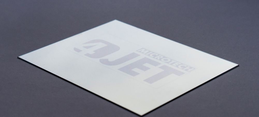
Laser Thin-Film Processing
As a leading supplier of industrial laser processing machines, we understand the crucial role of precision and reliability in modern manufacturing. Among the advanced techniques that are reshaping the boundaries of microfabrication, laser thin-film patterning stands out for its unmatched versatility and accuracy. This cutting-edge technology allows manufacturers to selectively remove or modify materials on thin films, enabling the creation of intricate patterns and high-resolution features without the need for physical masks or complex lithography processes.
How Laser Thin-Film Processing Works
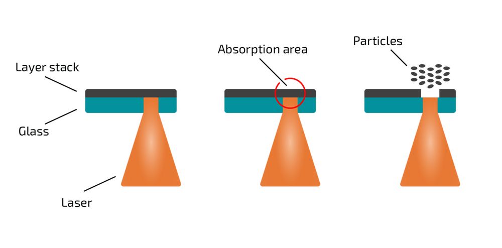
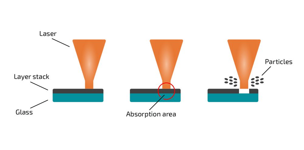
Laser thin-film processing (also patterning, structuring) is a highly precise method used to selectively remove or modify material on thin films deposited on various substrates. This is achieved using a focused laser beam that interacts with the material to either ablate, melt, or induce localized changes without affecting the surrounding regions.
Principle of Operation
Laser-Material Interaction:
- A focused laser beam, typically with wavelengths in the UV (355 nm), visible (532 nm), or infrared (1064 nm) range, is directed onto the thin film.
- The energy from the laser is absorbed by the thin-film material, resulting in localized heating.
- Depending on the energy density and the film's thermal and optical properties, this interaction can cause:
- Ablation (material removal through vaporization or sublimation),
- Melting and Re-solidification (changing surface properties without complete removal),
- Photo-induced Modification (alteration of chemical structure or crystallinity).
Scanning and Pattern Formation
- A computer-controlled scanning system (like galvanometer mirrors or precision stages) directs the laser beam along predefined paths.
- This enables the creation of complex geometries and micro-patterns with sub-micrometer precision.
Material Ejection and Debris Control:
- In ablation, material is ejected as vapor or particulates. Effective fume extraction and shielding can prevent contamination.
- In precise applications, gas-assisted removal is used to prevent redeposition.
Key Advantages of Laser Thin-Film Patterning
Types of Thin-Films Processed
Laser thin-film patterning is compatible with a wide range of materials, including:
| Category | Material | Applications |
|---|---|---|
| Metals | Gold (Au), Silver (Ag), Copper (Cu), Aluminum (Al), Nickel (Ni) | Automotive, Architecture, Microelectronics, interconnects and sensors. |
| Dielectrics and Oxides | Silicon Dioxide (SiO₂), Silicon Nitride (Si₃N₄), Aluminum Oxide (Al₂O₃), Perovskites | Photovoltaics, MEMS devices and micro-optics. |
| Transparent Conductive Oxides (TCOs) | Indium Tin Oxide (ITO), Aluminum Zinc Oxide (AZO) | Photovoltaics, display technology, touch panels and flexible electronics. |
| Polymers | Polyimide (PI), Polyethylene Terephthalate (PET), Polymethyl Methacrylate (PMMA) | Flexible circuits, microfluidics and biomedical devices. |
| Organic Films | Organic LEDs (OLEDs), organic photovoltaic cells | OLED Lighting, flexible displays and solar panels. |
| Semiconductors | Amorphous Silicon (a-Si), Cadmium Telluride (CdTe), Copper Indium Gallium Selenide (CIGS) | Photovoltaics and thin-film transistors (TFTs). |
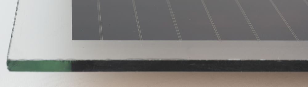
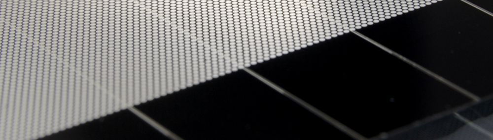
Laser Scribing of Thin-Films Enables Higher Efficiency in Photovoltaic Modules
Laser ablation of thin-films is pivotal in enhancing the efficiency of photovoltaic (PV) modules through precise structuring and interconnection. The following key improvements are enabled by laser processing:
In thin-film solar cells, the first laser scribing step (P1) creates isolation trenches between individual cells. This isolation prevents electrical short circuits and ensures that each cell operates independently, optimizing energy harvest.
The P2 step establishes electrical connections between the front and back electrodes without additional processing steps. P3 scribing isolates these connections, ensuring clean segmentation with minimal overlap.
This precise patterning reduces electrical losses and improves current flow.
Traditional mechanical methods often introduce shadowing on the active area. Laser scribing is non-contact and highly focused, minimizing shading and maximizing the light-capturing surface.
Laser patterning can minimize edge defects and recombination sites, which are typical loss mechanisms in thin-film solar cells.
Laser-based processing is not only faster but also seamlessly integrates into production lines, supporting high throughput without compromising precision.
The technology supports various photovoltaic materials, including CdTe, CIGS, and Perovskite, enhancing its application across different market segments.
By leveraging our advanced laser processing machines, PV manufacturers can achieve cleaner scribing, higher module efficiencies, and more reliable performance across varying environmental conditions.
Laser Edge Deletion and Laser Decoating Enable Higher Production Efficiency
Laser ablation of functional coatings on windshields, sunroofs and architectural glass can serve different purposes, like electrical isolation in the case of edge deletion or locally restoring transparency for sensors and HF communication. Laser processing enables the following significant improvements:
Compared to mechanical processing, laser processing does not involve mechanical tool wear. This keeps the processing quality consistently high.
Ablation products are removed directly by the highly efficient extraction system. This eliminates the need for cleaning the substrate after laser processing in most cases.
Due to the high flexibility of laser processes, the variety of possible laser sources and beam shaping, short cycle times or high process quality can be achieved. For large area decoating or edge deletion, kilowatt laser sources are used, to maximize throughput.
Due to the high flexibility of laser processes, you can process different substrate formats without mechanical changes
The high flexibility of laser processing in combination with our unique software enables you to create or adapt recipes with minimal effort.
Due to noncontact processing, the substrate will not be damaged.
By leveraging our advanced laser processing machines, your product can achieve cleaner structures and surfaces, higher production efficiency, and a more reliable performance across varying environmental conditions.
Driving Innovation with Laser Precision
Our laser processing machines are engineered with cutting-edge features to meet the evolving demands of modern manufacturing:
As global demand for thinner, lighter, and more efficient electronic devices continues to grow, manufacturers are turning to laser thin-film patterning as the key to staying competitive.
Our laser solutions are designed to push the boundaries of what’s possible – enabling faster time to market, lower production costs, and superior product reliability.
Whether you are developing the next generation of wearable sensors, high-efficiency solar panels, or flexible displays, our expertise and cutting-edge laser systems will empower you to achieve precision at scale.
Discover how our laser thin film patterning solutions can transform your manufacturing process. Contact us today to learn more about our industrial-grade laser processing equipment.


