

Semiconductor
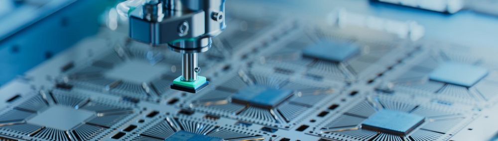
Laser Micromachining Solutions for Glass and Wafer Processing in the Semiconductor Industry
We deliver high-precision laser solutions for cutting, drilling, and microstructuring of glass, compound semiconductors, and wafer substrates – enabling advanced packaging, MEMS, and wafer-level applications with cleanroom-ready performance.
Laser Micromachining Solutions for Advanced Semiconductor and Glass Processing
As semiconductor architectures evolve toward heterogeneous integration, wafer-level optics, and 3D packaging, glass has emerged as a critical material. Its superior thermal stability, dielectric properties, and flatness make it indispensable for interposers, carrier wafers, MEMS, and photonic integration.
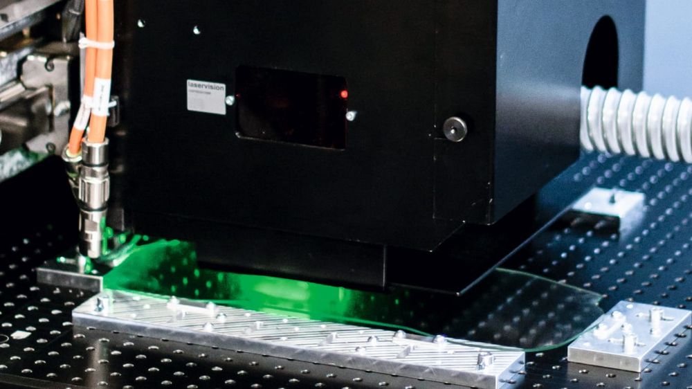
Our contactless laser micromachining systems support precise, scalable processing of thin and thick glass substrates, compound semiconductors, and functional coatings. Whether creating through-glass vias (TGVs), dicing fragile wafers, or structuring photonic features, our laser systems enable crack-free, contamination-free processes with sub-micron accuracy.
From R&D labs to high-volume fabs, our cleanroom-compatible platforms support backend wafer processing, advanced packaging, and optoelectronic integration across the semiconductor value chain.
Key Technical Features for Semiconductor Glass and Wafer Processing:
Key Applications & Our Capabilities
Dicing & Separation of Wafers and Glass Panels Processing of Compound Semiconductor Materials Drilling of Through-Glass Vias (TGVs) Wafer Structuring for MEMS & Photonics Drilling of Gas Distribution “Showerhead” Plates for Semiconductor Wafer Processing Edge Isolation and Functional Surface Treatment Wafer Edge Processing & Notching Coating Patterning & Selective Layer Removal
Dicing & Separation of Wafers and Glass Panels
Applications:
- Dicing of glass interposers, sensor substrates, and laminated wafer stacks
- Clean singulation of borosilicate, fused silica, and ultra-thin wafers (<50 µm)
- Ideal for borosilicate, fused silica, or ultra-thin glass wafers up to 300 mm
4JET Technology Fit:
- Bessel beam laser cutting for chip-free, debris-free separation for delicate substrates
4JET Solution:
- High-throughput, crack-free laser dicing with low kerf and superior edge strength – no post-polishing required
4JET Platforms:
Processing of Compound Semiconductor Materials
Applications:
- Cutting and structuring of GaAs, InP, SiC, and other brittle materials
- Applied in photonics, RF, power, and IR sensing applications
4JET Technology Fit:
- USP laser processing adapted for brittle and high-value materials with thermal control
4JET Solution:
- High-yield, low-damage processing for expensive, high-performance wafers
4JET Platforms:
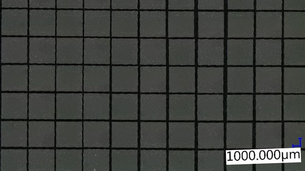
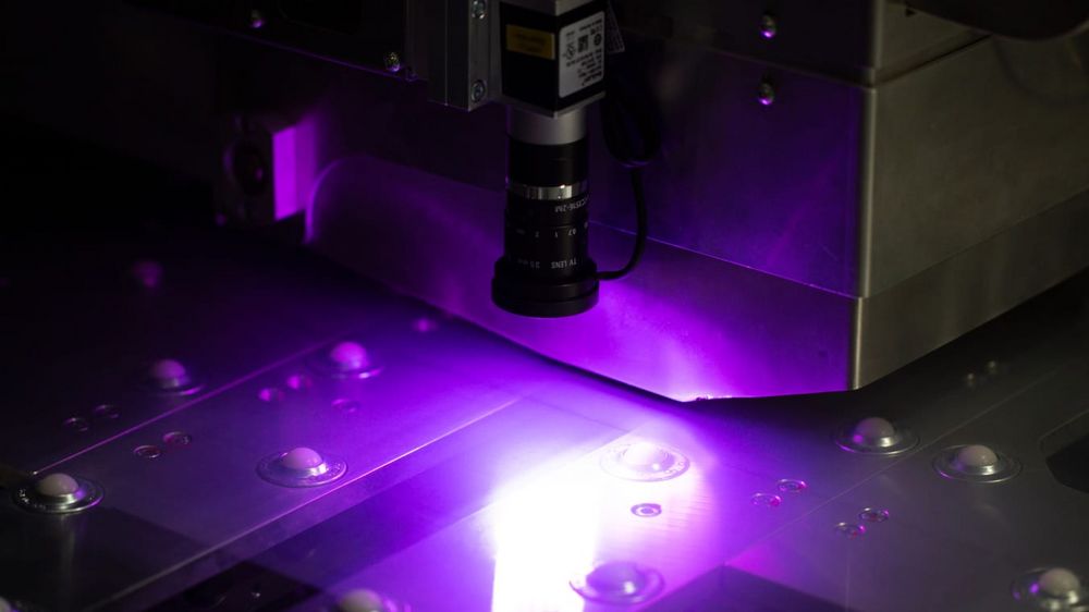
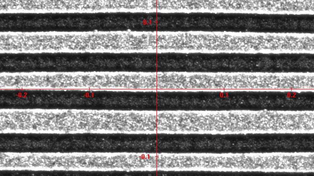
Drilling of Through-Glass Vias (TGVs)
Applications:
- Vertical interconnects in glass interposers and RF packages
- MEMS sensor channels and high-density via arrays
4JET Technology Fit:
- High-aspect-ratio laser drilling with micron precision
4JET Solution:
- Clean, crack-free conical or cylindrical through-glass vias (TGVs) with high aspect ratios and dimensional accuracy – scalable for panel and wafer-level formats in cleanroom environments
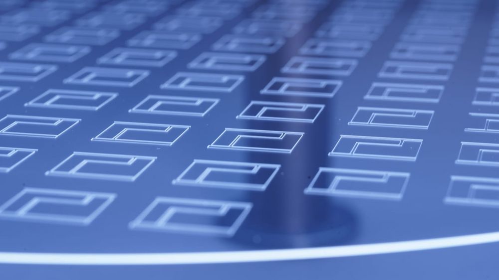
Wafer Structuring for MEMS & Photonics
Applications:
- Micromachining of cavities, gratings, microchannels, or optical features
- Applied in LIDAR, silicon photonics, and bioMEMS devices
4JET Technology Fit:
- USP laser structuring for complex 2.5D/3D topographies
4JET Solution:
- High-precision, flexible laser structuring tailored for MEMS and photonics device architectures
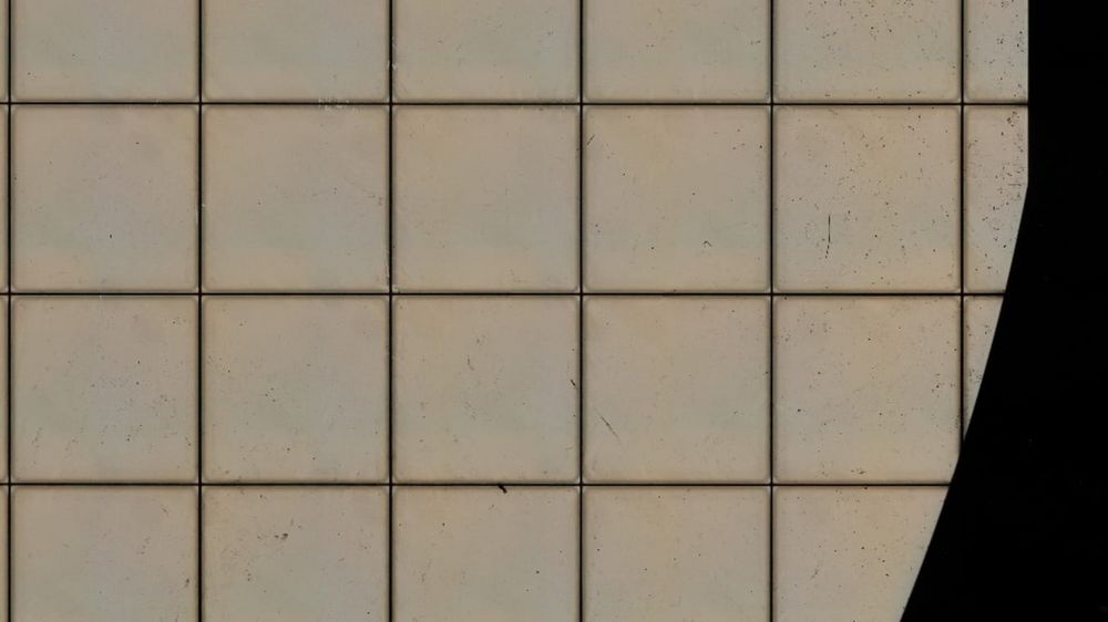
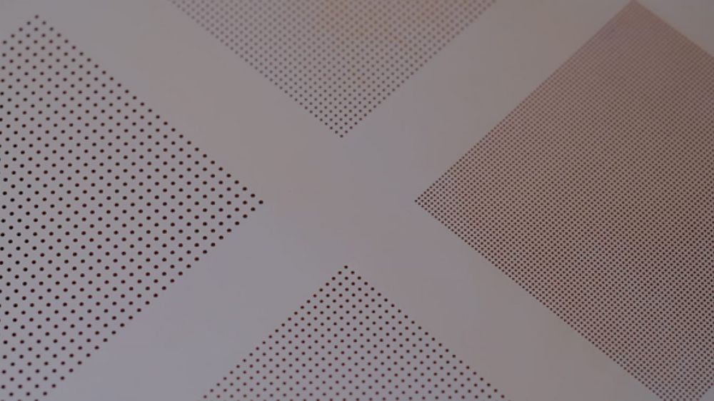
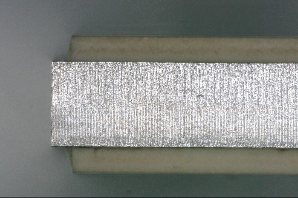
Drilling of Gas Distribution “Showerhead” Plates for Semiconductor Wafer Processing
Applications:
- Fabrication of gas distribution plates (showerheads) used in plasma etch, CVD, and ALD equipment
- High-density arrays of high-aspect-ratio sub-mm holes in thick borosilicate or fused silica glass
- Critical for uniform gas flow and plasma distribution across wafer surfaces in vacuum process chambers
4JET Technology Fit:
- Ultrashort pulse (USP) laser drilling with optimized parameters for deep, narrow features and smooth sidewalls
4JET Solution:
- Precision drilling of hundreds to thousands of tapered or cylindrical holes with aspect ratios >10:1
- Consistent hole diameter, roundness, and alignment, with no microcracks, debris, or backside chipping
- Compatible with cleanroom automation and wafer-scale plates up to 300 mm or larger
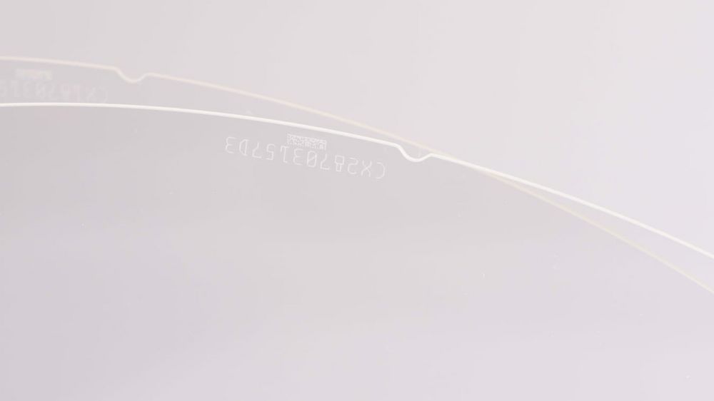
Edge Isolation and Functional Surface Treatment
Applications:
- Glass edge processing for alignment, bonding, or optical performance
- Surface tuning for bonding or dielectric control
4JET Technology Fit:
- Localized ablation or micro-texturing with sub-micron resolution
4JET Solution:
- Contactless isolation zones that support optical precision and electrical insulation
Wafer Edge Processing & Notching
Applications:
- Edge trimming and notching for automated handling, fiducial alignment, or packaging
4JET Technology Fit:
- Stress-free laser removal without wafer cracking or particle release
4JET Solution:
- Precise edge shaping – ideal for high-value MEMS or optical wafers
4JET Platforms:
Coating Patterning & Selective Layer Removal
Applications:
- Selective removal of functional or protective coatings (e.g., ITO, metals, dielectrics)
- Removal of passivation layers, thin films, or functional coatings (e.g., metals, dielectrics)
- Exposure of contact pads or bonding zones on wafer surfaces
- Applied to optoelectronics, MEMS sensors, or photonic circuits
4JET Technology Fit:
- High-resolution ablation with minimal thermal effect
4JET Solution:
- Consistent, maskless removal in multilayer glass or compound semiconductor stacks
Dicing of GlassCore Panels
Applications:
Separation of GlassCore panels (ex. 510mm x 515mm) with both side ABF stack into individual chiplets
4JET Technology Fit:
Laser dicing by IP protected EnP (Enhanced nanoPerforation) with CO2 or mechanical Separation
4JET Solution:
Adapted EnP optics for cutting through narrow ABF trenches providing chipping and crack free devices with highest bending strength. 4JET provides full inline solutions with EFEM interface for highest throughput in 24/7 production
Why 4JET?
Proven in MEMS, RF, photonics, and wafer-level packaging applications
Sub-micron laser accuracy with no mechanical tool wear or contact
Cleanroom-ready systems for backend integration and automation
Trusted partner from feasibility to volume production
Need Laser Precision in Glass Wafer Processing?
Speak with our semiconductor experts to explore integration of laser-based glass processing in your fab or packaging line.
Enabling Capabilities Across All Semiconductor Applications

Semiconductor manufacturing requires ultra-precise, contamination-free laser processing solutions that handle fragile wafers, glass carriers, and compound semiconductor materials with high throughput and repeatability. Our systems deliver robust performance, smart automation, and comprehensive support to meet these demanding needs.
Core4 Software Platform Global Services & SupportAutomation Integration
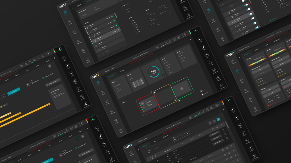
Core4 Software Platform
At the heart of every 4JET laser system, Core4 integrates advanced automation, machine vision, and process controls optimized for semiconductor fabrication.
- Modular and customizable software architecture with an intuitive UI
- AI-powered vision for real-time defect detection and alignment correction
- Seamless integration with factory automation and MES systems
- Continuous updates supported by a dedicated team of 20+ developers ensuring stability and scalability
Global Services & Support
Comprehensive support network for semiconductor fabs and assembly lines worldwide:
- Remote diagnostics, software support, and process optimization
- On-site training, preventive maintenance, and repair services
- Expert application consulting to tailor solutions for unique semiconductor processes
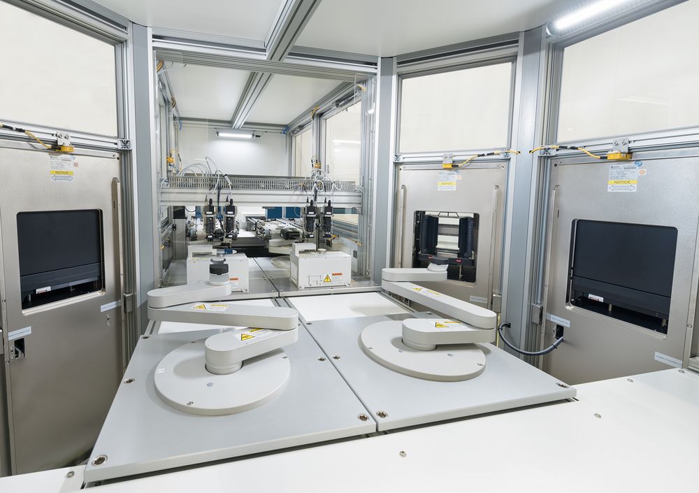
Automation Integration
Seamless integration into semiconductor manufacturing lines:
- Robotic wafer handling and cleanroom-compatible automation interfaces
- Support for high-throughput, multi-step process flows
- Customizable interfaces for metrology, alignment, and packaging stations
Need Laser Precision in Glass Wafer Processing?
Speak with our semiconductor experts to explore integration of laser-based glass processing in your fab or packaging line.


