

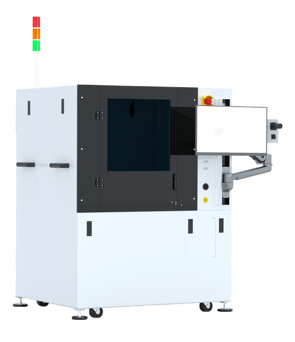
Wafer Dicing – Precise Scribe & Break with the DTX 200 NX
Precise wafer singulation is a critical step in the production of modern microtechnology. Whether in optics, sensor manufacturing, or general wafer processing: clean, low-stress break edges and maximum repeatability are essential.
With the DTX 200 NX, we offer a mechanical "scribe & break" system specifically designed for brittle materials – precise, reliable, and highly flexible.
What is Wafer Dicing?
The term wafer dicing refers to the process of separating semiconductor wafers or substrate carriers into individual chips or components. Depending on the material, different dicing technologies are used – including mechanical sawing (wafer saws), laser processing, or the so-called Scribe & Break method.
Especially for delicately coated substrates or brittle materials, the Scribe & Break technique offers a particularly gentle and process-safe alternative.
DTX 200 NX – Precision for Brittle Materials
The DTX 200 NX (derived from the Dynatex DTX-200) is a highly advanced tool for the mechanical singulation of brittle materials.
Using a dry dicing process, the system performs precise scribing and controlled breaking, enabling stress-free wafer separation with minimal microcracks – ideal for applications with strict edge quality requirements.
The DTX 200 NX supports both manual and automated operation, making it perfectly suited for R&D, prototyping, and small to mid-scale production environments.
Our dry dicing system offers an innovative solution for the precise separation of sensitive materials – without thermal load and without water consumption. Using laser- or diamond-based scribing technologies, you achieve maximum efficiency, top cutting quality, and flexible production for wafers up to 200 mm in diameter.
Your Key Benefits at a Glance:
Whether in semiconductors, MEMS, or optoelectronics – our DTX 200 NX dry dicing system combines precision, productivity, and sustainability.
Versatile Applications
As a mechanical complement to our laser-based dicing solutions – such as the PEARL 400S WD – the DTX 200 NX in its break-only configuration offers maximum flexibility for wafer processing.
Customers relying on mechanical dry dicing and breaking will find a robust and versatile solution for a wide range of applications:
- Dicing of glass wafers for semiconductors and optical systems
- MEMS and biomedical devices
- RFICs, Si photonics, and III-V chips
- Laser diode array separation
- LED substrates (break-only use)
- Singulation of wafers for microfluidic systems
- Structuring of thin glass wafers for sensor applications
Learn more about the Scribe & Break process, the laser cutting method, and discover our advanced laser dicing solutions with the PEARL 400S.
FAQ
- Stress-free breaking without thermal effects – ideal for temperature-sensitive components
- Precise break edges with no material loss
- Low to no particle generation – excellent for cleanroom environments
- No mechanical friction or heat, protecting delicate surface layers
- High repeatability, even for small batches
- Cost-effective and simple process
- Only suitable for materials that allow for clean breaking
- Microcracks may occur with certain sensitive layers or materials
- Not suitable for complex geometries, such as curved cuts
Yes! With the appropriate configuration, the DTX 200 NX enables contactless breaking before or after the application of sensitive coatings. Active and structured surfaces remain completely untouched – ensuring maximum process safety, especially for optoelectronic components or biomedical chips.
Absolutely. In combination with our nanoPerforation laser systems, such as the Pearl 400S WD, a hybrid process becomes possible:
First, the laser precisely perforates the wafer structure. Then, the DTX 200 NX mechanically separates the chips along the laser lines
This approach combines design flexibility with material-friendly processing.
- Processes wafers up to 200 mm in diameter
- Supports small die formats and custom shapes
- Cycle time per break: approx. 1.5 seconds – ideal for efficient series production
The low-contact breaking process significantly minimizes particle generation:
- Little to no chipping
- Minimal residue
- Excellent cleanroom compatibility – improves yield and reduces cleaning effort
The DTX 200 NX is compatible with a wide range of brittle materials, including:
- Fused silica
- Borosilicate glass
- Sapphire
- Coated glass
- III-V substrates such as GaAs and InP
Ideal for complex requirements in semiconductor and optoelectronic manufacturing.
Yes – both!
- The Wizard mode and operator-guided workflows make it ideal for research and prototyping
- The system’s fully automated processing ensures scalability for volume production
- User-friendly touchscreen GUI
- Interactive assistant modes simplify setup and processing
- No special training required for basic operation – fast, easy onboarding, ideal for environments with changing staff
The optimal choice depends on substrate type, design complexity, and production volume.
For complex layouts or materials that require non-mechanical processing, laser dicing may be preferable. For cost-efficient, low-stress singulation of brittle materials, the DTX 200 NX excels.
Yes – the DTX 200 NX is successfully used in:
- Optoelectronic components such as photodiodes and modulators
- MEMS systems
- Biomedical glass-based devices
- RFICs and laser diode arrays
These applications demonstrate the system’s robustness and clean, high-precision performance.


